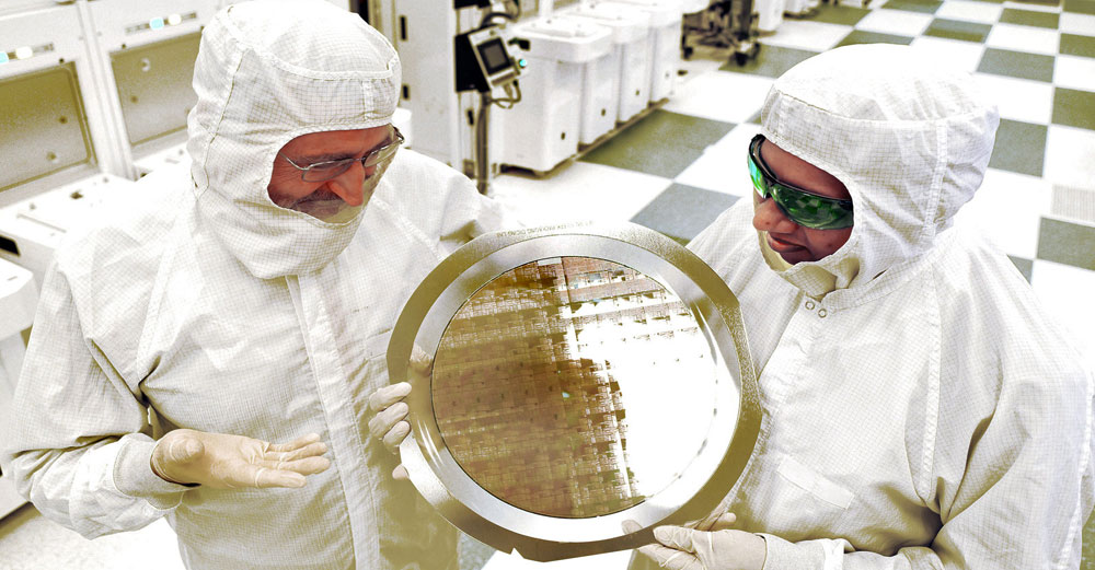
Recently, a partnership between IBM and SUNY Polytechnic Institute produced a ground-breaking innovation in computer technology. A new computer chip with 7-nanometer transistors, which are the smallest ever made by the industry, was revealed this week. Although this chip is very small, it’s also quite smart.
How small is 7nm? About 1/10,000th the width of a human hair. Even at less than half the size of the industry standard, this new chip is twice as powerful, with the potential to improve power and performance by 50% over previous chip models. The new chips could hold as many as 20 billion tiny transistor switches on a platform that fits on your fingernail! The more transistors that can be placed on a chip, the cheaper and better performing it can be.
This new tiny, 7nm technology development could mean great things for cloud computing, big data systems, and mobile technology that we all use daily. Whether active or passive, these are technologies and systems that are in use for personal or business needs in every corner of our world. And improved capabilities in storage, speed, and power consumption within these systems would be valued benefits for all of us.
Significant Developments
This isn’t the first breakthrough in computer and nanotechnology to come from SUNY Poly. Last year, the college unveiled the first-ever patterned 450mm wafer. At 18 inches across, these wafers could produce more than double the number of chips as on a 300mm wafer, the industry standard at the time of the announcement.
Now, these commercial 7nm chips are at least two years away from production, but this test chip is extremely significant for three reasons:
- it’s a working sub-10nm chip, a great achievement in size and density;
- it’s the first commercially viable sub-10nm chip to use silicon-germanium, a key product in low-cost, lightweight personal communication tools like smartphones, GPS systems, automobile tech, and other info/entertainment technologies, as the channel material;
- it appears to be the first commercially viable design produced with extreme ultraviolet (EUV) lithography.
The world of (nano)technology continues to move forward at SUNY. What will come next? Only time (and great minds) will tell.
Read more:
- http://www.theverge.com/2015/7/9/8919091/ibm-7nm-transistor-processor
- http://www.wsj.com/articles/ibm-reports-advances-in-shrinking-future-chips-1436414814?cb=logged0.08307621767744422
- http://arstechnica.co.uk/gadgets/2015/07/ibm-unveils-industrys-first-7nm-chip-moving-beyond-silicon/
- http://www.npr.org/sections/thetwo-way/2015/07/09/421477061/ibm-announces-breakthrough-in-chip-technology
- http://www-03.ibm.com/press/us/en/pressrelease/47301.wss


Really shows how far we’ve come at such an amazing rate. Can you believe that IBM fit 30 Billion transistors onto a chip the size of your nail? Very impressive!
Well thats great news to know that first of its kind has been made by sunny and hopefully they will do this kind of new technology in the coming future. I was thinking is this invention has something to do with nanotechnology because lots of new inventions has a huje efect of nanotechnology in them.